
Leading Companies in the Global Electronic Design Automation Market
Author:
Intellectual Market Insights Research
Published Date:
15 Jul 2026
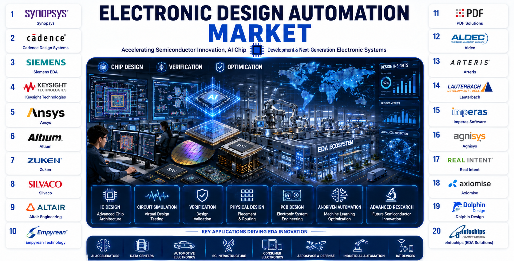
Top 10 Leading Companies in the Global Electronic Design Automation (EDA) Market 2026
Powering the Chips Behind the AI Revolution: EDA Industry Growth in 2026
The global semiconductor and electronics industry is undergoing one of its most profound technological transformations, and at the core of this revolution lies a critical enabler that rarely makes headlines: Electronic Design Automation. EDA encompasses the software tools, platforms, and methodologies that engineers rely on to design, simulate, verify, and manufacture semiconductor chips and complex electronic systems from the tiniest sensor ICs to the most advanced AI accelerator processors powering today's hyperscale data centers.
"The global Electronic Design Automation market was valued at approximately USD 19.15 billion in 2025 and is projected to reach USD 43.07 billion by 2034, expanding at a CAGR of 9.4% over the forecast period."
These figures reflect a fundamental reality: as chips grow exponentially more complex with modern SoCs containing tens of billions of transistors the EDA tools required to design, verify, and sign off on those chips must grow more sophisticated in parallel.
This article highlights the Top 10 Leading Companies in the Global Electronic Design Automation Market 2026, profiling organizations that are driving innovation, expanding AI-native design capabilities, and shaping the future of semiconductor chip design.
What is Electronic Design Automation (EDA)?
Electronic Design Automation refers to the category of software tools and methodologies engineers use to design, simulate, verify, and manufacture semiconductor chips and complex electronic systems. It spans a wide range of tools and workflow stages, including:
- RTL design and synthesis tools that translate hardware descriptions into gate-level logic
- Functional simulation and formal verification platforms that confirm chips behave as intended before tape-out
- IC physical design and place-and-route tools that convert logic into optimized silicon layouts
- Design rule checking (DRC) and layout-versus-schematic (LVS) verification
- Printed circuit board (PCB) design tools for system-level electronics
- Semiconductor IP blocks that allow designers to reuse pre-verified functional components rather than design from scratch
As chip complexity accelerates alongside the AI compute buildout, EDA has become an increasingly strategic and increasingly AI-driven layer of the global semiconductor value chain.
Global EDA Market Overview
|
Parameter |
Details |
|---|---|
|
Market Size (2025) |
USD 19.15 Billion |
|
Projected Market Size (2034) |
USD 43.07 Billion |
|
CAGR (2026–2034) |
9.4% |
|
Base Year |
2025 |
|
Forecast Period |
2025–2034 |
|
Leading Product Segment |
Semiconductor IP |
|
Leading Application Segment |
ASIC/SoC Design |
|
Fastest-Growing Region |
Asia-Pacific (CAGR of approximately 10.2%) |
|
Dominant Region (Revenue Share) |
North America (over 49.80% in 2025) |
|
Key Growth Drivers |
AI chip demand, 5G rollout, semiconductor complexity, cloud-based EDA adoption |
|
Key Challenges |
High R&D costs, export control restrictions, talent shortages, long design cycles |
|
Key Opportunities |
Chiplet/3D IC design, AI-powered EDA tools, China semiconductor self-sufficiency, cloud-native EDA platforms |
Several powerful forces are propelling the EDA market forward in 2026 and beyond. The relentless demand for AI compute infrastructure from training clusters to inference accelerators to edge AI chips is requiring entirely new generations of EDA tools capable of handling AI-optimized silicon architectures, chiplet-based designs, and 2.5D/3D IC integration.
The global 5G rollout and the approaching research phase of 6G are driving unprecedented investment in RF chip design, millimeter-wave antenna systems, and baseband processors, all of which demand highly specialized EDA capabilities spanning electromagnetic simulation, signal integrity analysis, and high-frequency circuit verification.
The transition to advanced process nodes from 7nm to 5nm, 3nm, and beyond is dramatically increasing design complexity and the engineering compute resources required to complete a single chip design, lengthening EDA tool engagement per design project and expanding total EDA spending per chip generation.
Government-backed semiconductor sovereignty initiatives around the world particularly the U.S. CHIPS and Science Act, Europe's Chips Act, and China's domestic semiconductor investment programs are funding new chip design activity and driving demand for EDA tools across geographies where limited prior chip design capacity existed.
Key Market Drivers
Several factors are contributing to the rapid growth of the global EDA market:
Surging AI Accelerator Demand
Surging global demand for AI accelerator chips is driving unprecedented complexity in semiconductor design and EDA tool requirements.
5G and Early-Stage 6G Investment
Rising adoption of 5G and early-stage 6G research is fueling massive RF and baseband chip design investment worldwide.
Expansion of Cloud-Based EDA Platforms
Rapid expansion of cloud-based EDA platforms is enabling distributed design teams and scalable compute access.
Automotive Electronics Growth
Growing adoption of EDA tools in automotive electronics for ADAS, EV powertrains, and functional safety-compliant chip design is expanding the addressable market.
AI-Native EDA Automation
Technological advancements in AI-native EDA automation including generative AI for RTL optimization, physical implementation, and verification are reshaping product roadmaps industry-wide.
Key Market Opportunities
- Expansion of EDA-as-a-Service and subscription-based cloud EDA models lowering barriers for fabless startups and academic institutions
- Premiumization of AI-driven EDA tools including autonomous design optimization, agentic chip design, and machine-learning verification platforms
- Chiplet and 3D IC design tooling innovation addressing the semiconductor industry's shift toward heterogeneous integration architectures
- Untapped market potential across India, Southeast Asia, and the Middle East as emerging semiconductor design ecosystems develop
- Integration of EDA tools with adjacent domains including TCAD, multiphysics simulation, and digital twin platforms into unified chip-to-system design workflows
Key Market Challenges
- High upfront R&D costs of developing and maintaining EDA tools capable of keeping pace with advancing semiconductor process nodes
- Shortage of skilled semiconductor design and EDA engineering talent globally, limiting addressable customer base growth
- Geopolitical export control restrictions fragmenting the global EDA market and accelerating China's domestic tool substitution
- Logistical challenges in managing EDA tool qualification, PDK integration, and foundry ecosystem compatibility across multi-vendor design flows
Why the EDA Market is Growing
1. Exponential Growth in Chip Design Complexity
Modern semiconductor devices contain billions of transistors on a single die, with today's leading-edge AI accelerators and mobile SoCs demanding design verification runs that can involve trillions of simulation cycles. Each new process node introduces additional design rules, parasitics, and verification challenges that require more sophisticated and more expensive EDA tooling to resolve.
2. AI Chip Demand and the Data Center Buildout
The explosive demand for AI training and inference compute is fueling an unprecedented surge in custom ASIC and chiplet design activity. Hyperscalers including Google, Amazon, Meta, and Microsoft are all designing proprietary AI accelerators, while a wave of AI chip startups is competing for market share all relying on advanced EDA tools to bring their designs to market.
3. Advanced Node Transitions and Chiplet Architectures
The semiconductor industry's shift toward chiplet-based designs and 2.5D/3D IC integration is introducing a new tier of EDA complexity. Managing multi-die systems, thermal interactions between chiplets, and the reliability of high-density inter-chiplet interconnects requires purpose-built EDA tools that did not exist at scale a decade ago.
4. Cloud-Based EDA Democratizing Access
Cloud-native EDA platforms commanded a dominant 67.1% revenue share in 2025, offering remote access to design software and computing resources without requiring massive on-premises infrastructure. The pay-as-you-go model is particularly attractive for fabless startups and small-to-mid-sized semiconductor companies with capital constraints, significantly expanding the addressable EDA market beyond established IDMs and large fabless firms.
5. 5G, IoT, and Automotive Electronics Growth
The global 5G rollout, rapid IoT device proliferation, and the electrification and autonomy transition in the automotive industry are collectively driving massive investment in new chip designs for each of these verticals. ADAS processors, vehicle-to-everything (V2X) communication chips, power management ICs for electric vehicles, and millimeter-wave 5G transceivers all require specialized EDA tool flows tailored to their respective design requirements.
6. Government Semiconductor Sovereignty Programs
National semiconductor investment programs across the United States, Europe, Japan, South Korea, and China are funding new chip design activity and, in several cases, directly supporting domestic EDA tool development. The U.S. CHIPS and Science Act alone is catalyzing billions of dollars in semiconductor manufacturing and design investment, expanding the pool of organizations designing chips and therefore demanding EDA tools.
Emerging Trends Shaping the Industry
The EDA industry is evolving rapidly with continuous technological advancements. Some of the most significant trends include:
- AI-native RTL optimization, floorplanning, and routing automation
- Chiplet and 3D IC design tooling for heterogeneous integration
- Cloud-native EDA platforms with elastic, pay-as-you-go compute access
- Design-Technology Co-Optimization (DTCO) linking TCAD and EDA workflows
- Automotive and functional safety-focused EDA (ISO 26262, AUTOSAR)
- EDA-as-a-Service and subscription-based consumption pricing models
- Agentic AI frameworks automating phases of the chip design flow
- Electromagnetic and signal integrity simulation for 5G/6G RF design
- Machine-learning-guided verification coverage prediction
- Expansion of domestic EDA tool development in China
These innovations are enabling faster, more automated, and more cost-efficient chip design cycles while creating new revenue opportunities for technology providers.
Top 10 Leading Companies in the Global Electronic Design Automation Market 2026
- Synopsys
- Cadence Design Systems
- Siemens EDA
- Keysight Technologies
- Ansys
- Altium
- Zuken
- Silvaco
- Altair Engineering
- Empyrean Technology
Company Profile
1. Synopsys
|
Category |
Details |
|---|---|
|
Company Name |
Synopsys |
|
Headquarters |
Mountain View, California, USA |
|
Founded |
1986 |
|
Industry Focus |
EDA Software, Semiconductor IP, Application Security |
|
Global Presence |
Global operations across North America, Europe, and Asia-Pacific, serving the world's leading semiconductor and systems companies |
|
Company Overview |
Synopsys is the world's largest provider of Electronic Design Automation software, semiconductor IP, and application security solutions. The company occupies an unmatched position at the center of the global semiconductor ecosystem, with its tools used by virtually every major chip designer in the world from hyperscale AI chip developers to automotive semiconductor suppliers. Synopsys' portfolio spans the full chip design flow, from RTL synthesis and functional verification to physical implementation, sign-off, and silicon lifecycle analytics. |
|
Key Products & Services |
Fusion Compiler (RTL-to-GDSII implementation), VCS and VC Formal (functional simulation and formal verification), IC Validator and StarRC (sign-off verification and extraction), PrimeTime (static timing analysis), a broad semiconductor IP portfolio spanning interface PHYs, processor IP and security IP, and Synopsys Software Integrity Group for application security testing |
|
Market Position |
Synopsys holds the largest revenue share in the global EDA market, with its tools embedded deeply in the design flows of TSMC, Samsung Foundry, Intel Foundry, and the world's leading fabless semiconductor companies. Its strong position in AI-driven design and verification automation has reinforced its market leadership through the current AI chip supercycle. |
|
Recent Developments |
Continued development of AI-driven EDA capabilities under the Synopsys.ai brand, including generative AI tools for chip design optimization. The company's previously announced merger with Ansys a landmark transaction that would combine EDA and multiphysics simulation remained subject to regulatory review as of mid-2026, with significant implications for the broader competitive landscape. |
|
Strategic Advantages |
Unmatched breadth across the full chip design flow, the largest semiconductor IP portfolio in the industry, deep customer relationships across every major semiconductor ecosystem participant, and early leadership in AI-powered EDA automation |
2. Cadence Design Systems
|
Category |
Details |
|---|---|
|
Company Name |
Cadence Design Systems |
|
Headquarters |
San Jose, California, USA |
|
Founded |
1988 |
|
Industry Focus |
IC Design, Verification, PCB Design, System Simulation, Semiconductor IP |
|
Global Presence |
Global operations across North America, Europe, and Asia-Pacific, with deep penetration at leading AI infrastructure and automotive semiconductor customers |
|
Company Overview |
Cadence Design Systems is one of the world's two dominant EDA providers, offering an integrated portfolio of software, hardware, and IP solutions for designing and verifying integrated circuits, printed circuit boards, and complex electronic systems. The company has successfully repositioned itself as an AI-driven computational software leader, with its Intelligent System Design strategy spanning from chip design to complete electromechanical system simulation. |
|
Key Products & Services |
Innovus Implementation System (physical chip design), Xcelium Logic Simulator and JasperGold Formal Verification (functional verification), Virtuoso Custom IC Design (analog and mixed-signal design), Allegro PCB Designer (board-level design), and a comprehensive IP portfolio |
|
Market Position |
Cadence holds the second-largest position in the global EDA market, with particularly strong penetration at hyperscale AI chip customers and leading automotive semiconductor suppliers. The company reported 17% year-over-year revenue growth guidance for 2026, driven by accelerating AI demand and record design backlog. |
|
Recent Developments |
Launch of the AgentStack agentic AI platform integrating ChipStack, ViraStack, and InnoStack AI Super Agents to automate key phases of the chip design flow. Core EDA revenue grew 18% year-over-year in Q1 2026, with hardware achieving a record quarter driven by AI and HPC customer demand. |
|
Strategic Advantages |
Best-in-class custom IC and analog design tools, strong AI-driven product innovation cadence, deep integration across digital, custom, and system design domains, and exceptional penetration at leading-edge semiconductor customers |
3. Siemens EDA
|
Category |
Details |
|---|---|
|
Company Name |
Siemens EDA |
|
Headquarters |
Wilsonville, Oregon, USA (division of Siemens Digital Industries Software) |
|
Founded |
1981 (as Mentor Graphics; acquired by Siemens in 2017) |
|
Industry Focus |
IC Design, PCB Design, System Verification, Digital Twin Integration |
|
Global Presence |
Global operations leveraging Siemens' broader industrial automation and digital industries footprint across more than 30 countries |
|
Company Overview |
Siemens EDA, formerly known as Mentor Graphics, is the third major pillar of the global EDA industry. Operating as a division under Siemens Digital Industries Software, the company brings together a legacy of EDA tool innovation with Siemens' vast industrial automation, digital twin, and manufacturing software ecosystem. This unique positioning allows Siemens EDA to serve not only chip designers but also system-level electronics engineers and manufacturing organizations seeking to integrate design and production workflows. |
|
Key Products & Services |
Calibre platform (IC physical verification and mask data preparation), Questa (functional simulation and formal verification), Xpedition and PADS (PCB and system-level electronics design), Capital (automotive electrical and electronic systems engineering), and Tessent (design-for-test and silicon lifecycle management) |
|
Market Position |
Siemens EDA holds a strong third-place position in the global EDA market, with particular strength in PCB and system-level electronics design, automotive electrical systems engineering, and IC physical verification. Its Calibre DRC platform is the de facto standard for physical verification at leading foundries including TSMC, Samsung, and Intel Foundry. |
|
Recent Developments |
In June 2025, Siemens Digital Industries Software introduced purpose-built EDA tools Innovator 3D IC and Calibre 3D Stacking to address the growing demand for chiplet-based 3D IC design and verification. Continued integration of AI capabilities across the Siemens EDA portfolio and expansion of its automotive systems engineering software. |
|
Strategic Advantages |
The industry-standard Calibre physical verification platform, unmatched breadth across IC design, PCB, and automotive systems engineering, deep integration with Siemens' manufacturing and digital twin software, and the ability to serve system-level electronics design workflows well beyond chip-level EDA |
4. Keysight Technologies
|
Category |
Details |
|---|---|
|
Company Name |
Keysight Technologies |
|
Headquarters |
Santa Rosa, California, USA |
|
Founded |
1983 (as EEsof; became Keysight's PathWave Design division following Keysight's 2014 spin-off from Agilent Technologies) |
|
Industry Focus |
EDA Software (RF/Microwave, High-Speed Digital, Circuit & System Simulation), integrated with Test & Measurement |
|
Global Presence |
Global operations serving telecommunications, aerospace & defense, automotive, and semiconductor customers worldwide |
|
Company Overview |
Keysight Technologies delivers EDA software through its PathWave Design division (formerly branded EEsof), focused on RF/microwave, high-speed digital, and signal integrity design. Through PathWave Design, Keysight provides Electronic Design Automation software to support high-speed product development, serving industries such as telecommunications, aerospace, defense, and automotive. Bitscale A distinguishing strength of Keysight's EDA business is its integration with the company's decades-long legacy in electronic test and measurement instrumentation, allowing simulation results to be validated directly against real-world measurement data. |
|
Key Products & Services |
PathWave Advanced Design System (ADS) for RF, microwave, and high-speed digital design; PathWave RFPro for 3D electromagnetic simulation; SystemVue for system-level wireless design; Genesys for RF circuit design; and device modeling tools for compound semiconductor and RF component design |
|
Market Position |
Keysight is recognized as a leading EDA vendor in the RF/microwave and high-speed digital design segment, named alongside Synopsys, Cadence, Siemens EDA, Ansys, and Zuken as a principal EDA competitor in industry filings. Its tools are widely used across wireless communications, aerospace/defense, and semiconductor device design. |
|
Recent Developments |
Continued rollout of AI/ML-enriched workflows and high-performance computation for digital twins and RF system optimization; deeper integration of measurement data into simulation to accelerate design-space exploration and standards-compliance automation; expanded support for advanced interconnect standards such as UCIe chiplet architectures; and early expansion into emerging applications including quantum hardware design. |
|
Strategic Advantages |
Unique integration of measurement and test data into the simulation environment, decades of RF/microwave design leadership, strong position in wireless and high-speed digital markets, and the backing of Keysight's broader test-and-measurement business and R&D infrastructure |
5. Ansys
|
Category |
Details |
|---|---|
|
Company Name |
Ansys |
|
Headquarters |
Canonsburg, Pennsylvania, United States |
|
Founded |
1970 |
|
Industry Focus |
CAE / Multiphysics Engineering Simulation Software (electromagnetic, structural, thermal, and fluid simulation) |
|
Global Presence |
Global operations serving aerospace, automotive, electronics, semiconductor, and industrial customers worldwide |
|
Company Overview |
Ansys is the global leader in engineering simulation, offering the best and broadest portfolio of engineering simulation software to help the world's most innovative companies deliver radically improved products Keysight spanning electromagnetic, structural, thermal, and fluid domains. Note: Unlike the other companies profiled here, Ansys is no longer an independent EDA vendor on July 17, 2025, the company became a subsidiary of Synopsys Wikipedia following a $35 billion acquisition, positioning the combined company to address an expanded $31 billion total addressable market spanning silicon design, IP, and simulation and analysis. |
|
Key Products & Services |
Ansys HFSS (3D electromagnetic simulation), Ansys SIwave (signal and power integrity), Ansys RedHawk-SC (chip power/thermal analysis), Ansys Icepak (thermal simulation), Ansys Mechanical (structural simulation), and Ansys Fluent (computational fluid dynamics) |
|
Market Position |
Ansys has established itself as the dominant force in simulation software, now integrated into Synopsys's silicon-to-systems platform following completion of the acquisition. |
|
Recent Developments |
The Synopsys-Ansys deal was finalized on July 17, 2025, after 18 months of negotiations and regulatory scrutiny, combining Synopsys' EDA and semiconductor IP leadership with Ansys' multi-physics simulation capabilities. Forbes Chinese regulatory approval came with conditions requiring Synopsys to divest its optical and photonic-device simulation business, while Ansys was required to divest its power consumption-analysis software operations, along with 10-year behavioral remedies requiring the companies to honor existing customer contracts. Technology Magazine Early integration efforts are focused on embedding multi-physics capabilities into Synopsys' chip design and verification tools, with the first joint solutions expected in the first half of 2026. |
|
Strategic Advantages |
Unmatched breadth in multiphysics simulation across electromagnetic, structural, thermal, and fluid domains; deep integration now with Synopsys's EDA and semiconductor IP portfolio for full silicon-to-systems design; and established presence across aerospace, automotive, electronics, and industrial verticals |
Competitive Landscape
The global Electronic Design Automation market exhibits a highly concentrated competitive structure at the top, dominated by a small number of players Synopsys, Cadence Design Systems, and Siemens EDA that together command an estimated 60–70% of global EDA software revenue. Below this dominant tier, a broader field of specialized vendors addresses specific workflow niches, regional markets, and adjacent simulation domains.
The competitive landscape is shaped by several key dynamics:
The EDA Oligopoly and Its Limits
The dominance of Synopsys, Cadence, and Siemens EDA reflects decades of consolidation and the high switching costs inherent in EDA tool adoption. Semiconductor companies invest years of engineering effort in qualifying EDA tools for their design flows, PDK integrations, and foundry technology access, creating deep lock-in that is difficult for new entrants to overcome through product capability alone.
AI as the Next Competitive Frontier
Both Synopsys and Cadence have made substantial investments in AI-driven EDA capabilities, with Synopsys' Synopsys.ai and Cadence's Cadence.AI platforms representing competing visions for how machine learning will automate and optimize the chip design process. AI-driven physical implementation, verification prediction, and autonomous design space exploration are becoming critical competitive differentiators.
The Synopsys-Ansys Merger Implications
The proposed acquisition of Ansys by Synopsys if completed would create an EDA and multiphysics simulation combination with no direct competitor in scope or scale, potentially reshaping competitive dynamics across both markets. Regulatory review outcomes will be watched closely by the entire semiconductor EDA ecosystem.
China's Domestic EDA Development
Export controls restricting Chinese semiconductor companies' access to foreign EDA tools have created an unprecedented strategic opening for domestic Chinese EDA vendors, led by Empyrean Technology. While current domestic tools cover only portions of the full design flow with tool maturity gaps versus U.S. leaders, the scale of government investment and policy pressure is creating a structurally distinct Chinese EDA sub-market that will increasingly develop on its own technology trajectory.
Cloud EDA Disruption
The shift toward cloud-native EDA platforms is introducing new competitive dynamics, as hyperscale cloud providers including AWS, Google Cloud, and Microsoft Azure are becoming important partners and potential disruptors in EDA tool delivery. Cloud-native EDA startups targeting specific design workflow stages represent an emerging competitive pressure on incumbent EDA vendors' traditionally on-premises delivery models.
Market Segmentation
By Tool Category
- RTL Design and Synthesis Tools
- Functional Simulation and Formal Verification Platforms
- IC Physical Design and Place-and-Route Tools
- Design Rule Checking (DRC) and Layout-Versus-Schematic (LVS) Verification
- PCB Design Tools
- Semiconductor IP Blocks
- TCAD and Multiphysics Simulation Tools
By Product Segment
- Semiconductor IP (leading segment)
- Digital Design and Verification
- Custom IC and Analog Design
- System Design and Analysis
By Application
- ASIC/SoC Design (leading segment)
- Automotive Electronics (ADAS, EV Powertrains, Functional Safety)
- 5G/6G RF and Baseband Chip Design
- AI Accelerator and Chiplet/3D IC Design
- PCB and System-Level Electronics
By Deployment Model
- On-Premises EDA
- Cloud-Native EDA (67.1% revenue share in 2025)
Regional Analysis
North America
North America dominates the global EDA market, capturing over 49.80% of global revenue in 2025. The region's dominance reflects the headquarters concentration of the world's three largest EDA vendors Synopsys, Cadence, and Keysight as well as the presence of the world's most productive fabless semiconductor ecosystem, centered in Silicon Valley and extending across the United States. The U.S. CHIPS and Science Act is catalyzing further domestic semiconductor design investment, expanding the North American EDA customer base beyond its already substantial scale.
Asia-Pacific
Asia-Pacific is the fastest-growing EDA market region, projected to register a CAGR of approximately 10.2% through 2034 above the global average. The region's semiconductor powerhouses Taiwan, South Korea, Japan, and China are all investing heavily in advanced chip R&D. Taiwan's TSMC and South Korea's Samsung, as the world's two leading foundries, drive massive EDA tool adoption as the volume and complexity of chips designed and manufactured on their processes grows. China represents a uniquely complex dynamic, with government-driven domestic semiconductor investment creating EDA demand while simultaneously pushing toward domestic tool substitution.
Europe
Europe maintains a specialized but important role in the global EDA ecosystem, anchored by Siemens EDA's strong European heritage and the region's automotive semiconductor sector one of the most EDA-intensive end markets given the complexity of modern vehicle electronic architectures. Countries including Germany, France, and the Netherlands host significant semiconductor design and automotive electronics engineering activity, with EDA tool adoption driven by ADAS, electric vehicle powertrain, and industrial automation chip design projects.
Latin America
Latin America represents a smaller but developing EDA market, with emerging semiconductor design ecosystems in Brazil and Mexico supported by growing technology sector investment and expanding engineering talent bases. Adoption of EDA tools in the region remains at an early stage relative to North America, Europe, and Asia-Pacific, though academic and government-supported chip design initiatives are creating early growth momentum.
Middle East and Africa
The Middle East and Africa represent early-stage EDA markets, with Israel serving as a notable exception hosting a disproportionately sophisticated semiconductor design ecosystem that is home to major chip design centers for Intel, Qualcomm, and numerous Israeli fabless startups. Gulf region investment in advanced technology ecosystems is creating nascent chip design activity that may expand EDA tool adoption over the forecast horizon.
Key Market Trends
- AI-native RTL optimization and automated floorplanning
- Machine-learning-guided routing and verification coverage prediction
- Chiplet and 3D IC design tooling for heterogeneous integration
- Cloud-native EDA platforms with elastic, pay-as-you-go compute
- Design-Technology Co-Optimization (DTCO) linking TCAD and EDA
- Automotive and functional safety EDA (ISO 26262, AUTOSAR)
- EDA-as-a-Service and subscription-based revenue models
- Agentic AI frameworks automating chip design phases
- Electromagnetic and signal integrity simulation for 5G/6G
- China's accelerating domestic EDA tool development
Future Outlook (2026–2034)
The global Electronic Design Automation market's trajectory toward approximately USD 43.07 billion by 2034 is supported by a convergence of durable structural tailwinds. The relentless march of Moore's Law even in its increasingly evolutionary rather than revolutionary form continues to drive chip design complexity upward with each new process node, requiring more sophisticated and more computationally intensive EDA tools to complete each design generation.
Key investment themes include the continued development of AI-native EDA platforms capable of autonomously optimizing portions of the chip design flow, growth in chiplet and 3D IC design tooling addressing the semiconductor industry's architectural shift toward heterogeneous integration, expansion of cloud-native EDA platform adoption across a broader customer base, and the maturation of China's domestic EDA ecosystem as geopolitical pressures accelerate domestic tool development.
For investors, the EDA market offers exposure to the secular growth of semiconductor complexity and design activity, with significant upside concentrated in companies that successfully leverage AI to compress design timelines and reduce engineering headcount requirements per chip design project. Leading companies Synopsys, Cadence, and Siemens EDA are likely to continue capturing the majority of EDA spending growth, while specialized vendors in high-frequency simulation, TCAD, and chiplet design tools offer more targeted exposure to fast-growing workflow sub-segments.
Frequently Asked Questions (FAQs)
1. What is Electronic Design Automation (EDA)?
EDA refers to the software tools, platforms, and methodologies engineers rely on to design, simulate, verify, and manufacture semiconductor chips and complex electronic systems.
2. Which companies are leading the global EDA market?
Leading companies include Synopsys, Cadence Design Systems, Siemens EDA, Keysight Technologies, Ansys, Altium, Zuken, Silvaco, Altair Engineering, and Empyrean Technology.
3. What factors are driving market growth?
AI chip demand and data center buildout, advanced node transitions and chiplet architecture complexity, 5G and 6G communications semiconductor investment, automotive electrification and ADAS chip design growth, government semiconductor sovereignty investment programs, and cloud-based EDA democratizing access to design tools are major growth drivers.
4. Which region dominates the EDA market?
North America leads the market with over 49.80% of global revenue in 2025, driven by the headquarters concentration of leading EDA vendors and the world's most productive fabless semiconductor ecosystem. Asia-Pacific is the fastest-growing region, projected at a CAGR of approximately 10.2%.
5. What is the forecast CAGR for the EDA market?
One widely cited estimate puts the CAGR at 9.4% from 2026 to 2034; other research providers' estimates generally range from approximately 7% to 10.2% depending on market scope and methodology.
6. What are the primary types of EDA tools?
Key categories include RTL synthesis and implementation tools, functional simulation and formal verification platforms, IC physical design and place-and-route tools, design rule checking and layout-versus-schematic verification, PCB design tools, semiconductor IP blocks, TCAD for device modeling, and multiphysics simulation tools for EM and thermal analysis.
7. What challenges does the EDA market face?
Key challenges include the high cost and long timelines of EDA tool R&D required to keep pace with advancing semiconductor process nodes, geopolitical export control restrictions affecting global EDA tool access and creating market fragmentation, talent shortages in semiconductor design engineering limiting the growth of the addressable EDA customer base, and the financial and operational complexity of the transition from perpetual to subscription licensing models.
8. What is cloud-based EDA?
Cloud-based EDA refers to the delivery of electronic design automation tools and computing resources through cloud platforms, enabling design teams to access EDA software and scale computational resources on demand without on-premises infrastructure investment. The cloud-based segment commanded a 67.1% revenue share in 2025 and is the fastest-growing deployment model in the EDA market.
9. How is AI impacting the EDA market?
AI and machine learning are being integrated throughout the chip design flow, enabling AI-assisted RTL optimization, automated physical implementation, machine-learning-guided verification coverage prediction, and early exploration of AI-driven autonomous chip design. Both Synopsys and Cadence have launched comprehensive AI-native EDA platforms, with agentic AI tools beginning to automate previously labor-intensive design tasks.
10. What investment opportunities exist in the EDA market?
Investment opportunities span AI-native EDA platform development, chiplet and 3D IC design tooling addressing the industry's architectural shift, cloud-native EDA delivery platforms expanding the addressable market, China domestic EDA ecosystem development, and specialized simulation vendors addressing high-frequency, TCAD, and automotive functional safety design workflows.
Conclusion
The global Electronic Design Automation market stands at a pivotal inflection point, transitioning from a tool-centric industry serving specialist chip designers to an AI-driven design automation platform market capable of compressing chip development timelines, reducing engineering resource requirements, and enabling a broader range of organizations to design advanced semiconductors. With a projected market size of approximately USD 43.07 billion by 2034 and sustained high-single-digit to low-double-digit growth, the sector offers compelling opportunities for semiconductor executives, engineering teams, investors, and technology buyers alike.
The top companies in the EDA market led by Synopsys, Cadence Design Systems, and Siemens EDA are not merely competing on tool feature sets. They are competing on the quality and depth of their AI-driven design automation capabilities, their ability to address the emerging complexity of chiplet and 3D IC design, and their success in transitioning customers to cloud-native, subscription-based EDA platforms that create more durable revenue relationships. The companies that successfully navigate the AI-native EDA transition while expanding their addressable market through cloud deployment will define the industry's leadership landscape through 2030 and beyond.
At the same time, the geopolitical bifurcation of the global semiconductor ecosystem driven by export controls and national semiconductor sovereignty initiatives is creating a structurally distinct Chinese EDA sub-market that will increasingly develop on its own trajectory, led by Empyrean Technology and supported by unprecedented levels of government investment. How this dynamic unfolds will be one of the defining competitive storylines of the global EDA industry through the latter half of this decade.