
FD-SOI Wafers Market: A Comprehensive Analysis of Size, Share, Applications, and Growth Opportunities Through 2031
Author:
Intellectual Market Insights Research
Published Date:
29 Jun 2026
FD-SOI Wafers Market: A Comprehensive Analysis of Size, Share, Applications, and Growth Opportunities Through 2031
Introduction:
The global semiconductor industry stands at a pivotal inflection point. As the limits of conventional bulk CMOS scaling become increasingly visible — characterized by mounting leakage currents, power density challenges, and escalating manufacturing costs at sub-10nm nodes — chipmakers and system integrators are turning to alternative process technologies that deliver compelling performance-per-watt advantages. Among these, Fully Depleted Silicon-on-Insulator, or FD-SOI, has emerged as one of the most strategically significant wafer substrate platforms of the current decade.
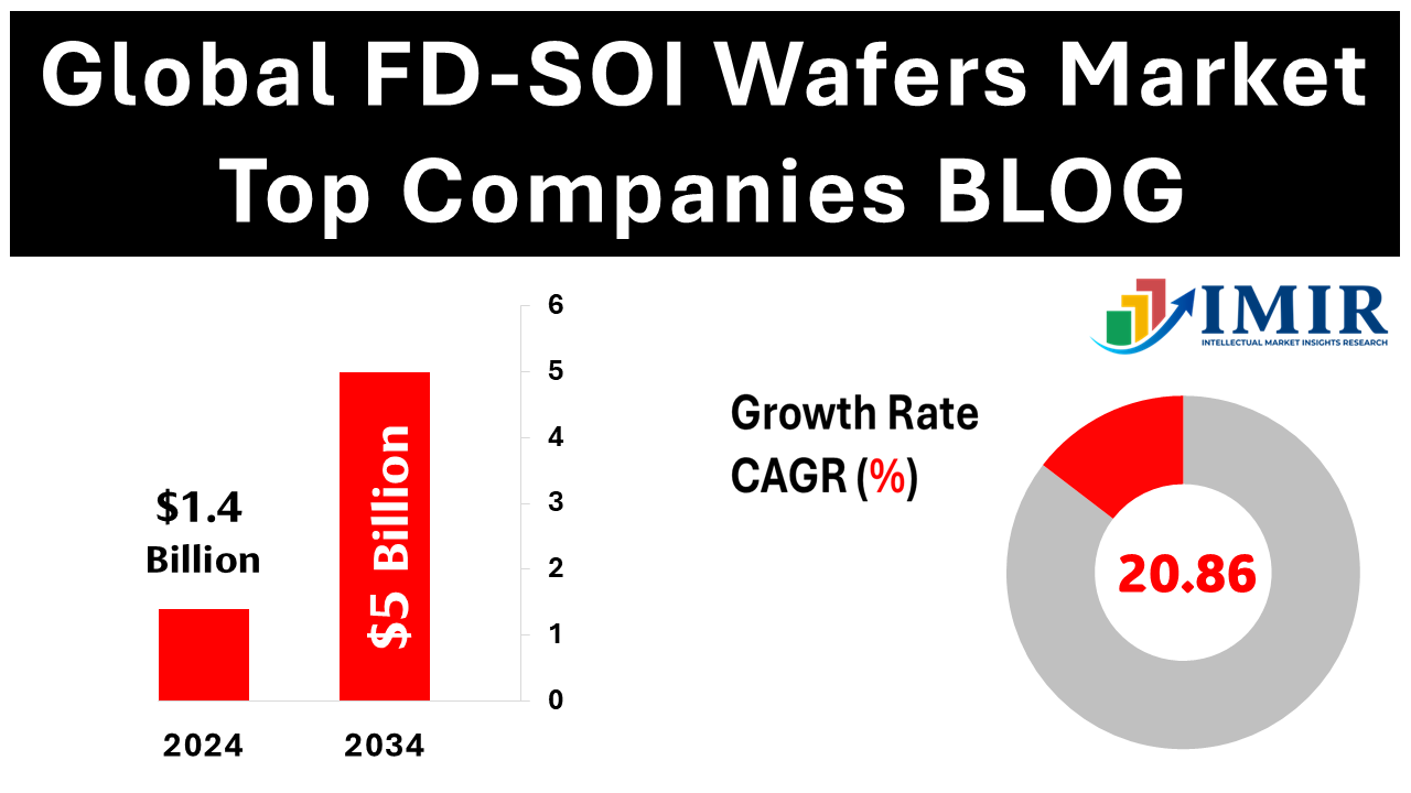
According to Intellectual Market Insights Research's dedicated FD-SOI Wafers Market report, the global market was valued at USD 616 million in 2022 and is on a trajectory to reach USD 2,189.41 million by 2031, expanding at a remarkable compound annual growth rate (CAGR) of 20.86% over the forecast period. These numbers place FD-SOI among the fastest-growing segments within the broader semiconductor industry reports landscape.
What makes FD-SOI particularly compelling is not simply the technology's intrinsic performance characteristics — which include dramatically reduced short-channel effects, near-zero body coefficient variability, and native back-biasing capabilities that allow dynamic voltage and frequency scaling — but rather the breadth of applications where these advantages translate into commercially meaningful differentiation. The technology's strongest footprints today are in 5G radio frequency (RF) front-end modules, advanced automotive microcontrollers and sensor fusion chips, IoT edge devices requiring ultra-low standby power, and wearable health monitors demanding milliwatt-class power budgets.
The industry landscape is shaped by a tightly controlled supply chain. Soitec in France dominates the engineered SOI substrate supply, partnering closely with key foundry champions including GlobalFoundries, STMicroelectronics, and Samsung Foundry, each of which offers their own FD-SOI process platforms targeting different application niches and node generations. On the wafer materials side, established silicon specialists — including Shin-Etsu Chemical, SUMCO Corporation, and Siltronic — provide the premium-grade silicon substrates that form the base layer of SOI wafer construction.
From a regional standpoint, North America currently holds the largest revenue share, supported by the density of fabless semiconductor design companies, defense and aerospace procurement, and strong university-industry R&D collaboration on advanced process platforms. Asia-Pacific, however, is expected to register the fastest CAGR through 2031, propelled by aggressive 5G infrastructure buildout in China, Japan's traditional strength in precision semiconductor materials, and South Korea's well-capitalized foundry ecosystem.
Across verticals, the application landscape is diversifying rapidly. Beyond its established position in smartphone RF switches and low-power microcontrollers, FD-SOI is now being actively evaluated for neuromorphic computing, quantum computing companion chips, satellite-grade mixed-signal integration, and next-generation radar-on-chip designs for advanced driver assistance systems (ADAS). As chip designers search for process platforms that offer meaningful differentiation without the capital expenditure burden of leading-edge FinFET nodes, FD-SOI's value proposition grows progressively stronger.
This article provides a comprehensive, data-driven analysis of the FD-SOI Wafers Market, covering technology fundamentals, key market segments, leading companies, regional dynamics, growth drivers, challenges, emerging opportunities, and the long-term outlook through 2031.
What Is FD-SOI Technology? A Technical Primer for Market Participants
The Silicon-on-Insulator Foundation
Silicon-on-Insulator (SOI) wafer technology places a thin layer of high-purity crystalline silicon on top of a buried oxide (BOX) layer, which in turn sits on a standard silicon substrate. This architecture fundamentally changes the electrical environment in which transistors operate: the buried oxide electrically isolates the active silicon layer from the bulk, suppressing parasitic currents, reducing junction capacitance, and enabling tighter electrostatic control over the transistor channel.
In the Fully Depleted variant — FD-SOI — the active silicon layer is thin enough (typically 5–7nm) that the transistor channel is fully depleted of free carriers at equilibrium. This eliminates the floating body effects and random dopant fluctuation that have long plagued partially depleted SOI devices, producing transistors with near-ideal subthreshold slopes and dramatically reduced threshold voltage variability. For chip designers, this translates into the ability to operate at lower supply voltages without sacrificing reliability or timing margins — a critical advantage in battery-powered and thermally constrained applications.
The technology also inherits the Silicon-on-Insulator market's unique back-biasing capability: by applying a voltage to the substrate beneath the BOX, designers can dynamically shift transistor threshold voltages on-the-fly, allowing a single chip to toggle between a high-performance mode during peak workloads and an ultra-low-leakage sleep mode during standby. This is a capability that conventional bulk CMOS simply cannot replicate without complex and area-expensive dual-threshold techniques.
FD-SOI Node Generations
The market currently spans three active node generations, each serving distinct application clusters:
28nm FD-SOI represents the most commercially mature and widely deployed node. ST's 28FD-X platform and GlobalFoundries' 22FDX remain the reference implementations. At 28nm, FD-SOI delivers leakage performance comparable to bulk 14nm FinFET at significantly lower manufacturing cost, making it attractive for cost-sensitive IoT sensors, wearables, automotive microcontrollers, and industrial edge devices.
22nm, 18nm, and 14nm FD-SOI nodes extend the technology's performance envelope, targeting more computationally intensive applications including 5G millimeter-wave baseband processing, advanced driver assistance system (ADAS) chips, and connectivity SoCs. These nodes offer further leakage reduction and higher maximum clock frequencies while retaining the back-biasing and low-variability advantages that define the FD-SOI platform.
12nm and 10nm FD-SOI represent the current frontier of the technology. Proponents argue these nodes can deliver performance within 15–20% of leading-edge 7nm FinFET while maintaining meaningful cost and power advantages for applications that don't require maximum computational density. Research programs at multiple universities and national labs continue to push FD-SOI toward sub-10nm dimensions using advanced gate-all-around structures built on SOI substrates.
Market Overview: Segments, Size, and Structural Dynamics
Market Segmentation by Wafer Type
The FD-SOI Wafers Market is segmented by node geometry, reflecting the technology maturity and application orientation of each process generation.
28nm Wafers hold the dominant volume share today. As the most commercially mature FD-SOI node, 28nm SOI wafer demand is driven by the large installed base of designs targeting IoT edge nodes, Bluetooth and Wi-Fi connectivity chips, microcontroller units (MCUs), and entry-level smartphone modems. Foundry capacity at this node is well-established, tooling is fully amortized, and design ecosystems are comprehensive. The 28nm SOI segment is expected to maintain strong volume through 2031 even as newer nodes attract incremental design starts.
22nm, 18nm, and 14nm Wafers represent the current primary growth engine of the FD-SOI market. This bracket captures high-value designs in 5G RF front-end modules, ADAS radar chips, advanced wearable health devices, and mixed-signal data converters. GlobalFoundries' 22FDX platform has achieved significant commercial traction in 5G and IoT applications. STMicroelectronics has positioned its 18nm FD-SOI variants for automotive and industrial customers requiring AEC-Q100 qualification and extended temperature operation. Revenue per wafer in this segment is meaningfully higher than 28nm, driving disproportionate value contribution to total market revenue.
12nm and 10nm Wafers remain an emerging and fast-growing segment. Volume is still relatively limited compared to established nodes, but design activity is accelerating, particularly for next-generation AI inference chips designed to operate within strict power envelopes, satellite communication processors, and ultra-high-frequency radar-on-chip components targeting autonomous vehicle sensing.
Market Segmentation by Application
The application landscape for FD-SOI spans eight major verticals, each with distinct demand drivers and growth characteristics.
5G and Radars constitute the single most commercially visible application for FD-SOI in the near term. RF-SOI and FD-SOI technology underpin the radio frequency switches, low-noise amplifiers, and power amplifiers embedded in smartphone 5G RF front-end modules. As global 5G subscriber counts continue to scale — driven by carrier investments tracked across Electronics & Telecommunication industry reports — demand for high-performance RF wafers continues to intensify. Beyond smartphones, FD-SOI's suitability for millimeter-wave radar signal processing makes it attractive for advanced automotive radar, satellite ground terminals, and defense electronic warfare applications.
Automotive applications represent a structural growth opportunity as the vehicle electronics content per unit climbs steeply with the electrification and autonomy megatrends. The Automotive Semiconductor Market is experiencing one of the most dramatic demand acceleration cycles in its history, and FD-SOI's combination of low-power operation, wide voltage scalability, and AEC-Q100 qualification suitability makes it well-positioned to capture a meaningful share of automotive MCU and SoC content. Applications include body control modules, gateway processors, ADAS domain controllers, and V2X communication chips.
Consumer Electronics represents a high-volume application where FD-SOI competes primarily on power efficiency in smartphones, tablets, smartwatches, and fitness trackers. The Smartwatch Chips Market is a particularly relevant proxy, as wearable application processors represent ideal FD-SOI target designs: constrained battery capacity, demanding computational tasks, and a need for always-on health-sensing functionality.
IoT and Wearables are perhaps the application area most naturally aligned with FD-SOI's core technological advantages. Connected sensors, edge inference chips, and wireless communication devices all benefit enormously from the ability to toggle between high-performance and ultra-low-leakage states using back-biasing. As the global IoT device installed base continues to scale, the cumulative demand for FD-SOI wafers from this segment is expected to be substantial.
Healthcare applications, including implantable medical devices, patient monitoring wearables, and diagnostic imaging ASICs, are increasingly adopting FD-SOI for its combination of ultra-low power operation and excellent single-event upset (SEU) immunity — a critical characteristic for radiation-hardened and medical-grade devices.
Industrial semiconductor applications, including programmable logic controllers, industrial Ethernet bridges, and motor drive controllers, benefit from FD-SOI's extended operating temperature range and supply voltage scalability. This is a steady, if less dramatic, demand segment.
Aerospace represents a specialized but high-value market. FD-SOI's inherent radiation hardness — a consequence of the buried oxide's charge trapping properties — makes it naturally suited for space-grade electronics where radiation tolerance is mandatory. Satellite processors, deep-space instrument controllers, and launch vehicle avionics represent active design areas.
Mobility encompasses a broad category of transportation-related applications spanning automotive telematics, fleet management chips, and emerging vehicle-to-infrastructure (V2I) communication processors.
Top Leading Companies in the Global FD-SOI Wafers Market
- Soitec
- Shin-Etsu Chemical Co., Ltd.
- SUMCO Corporation
- Okmetic Oy
- Silicon Valley Microelectronics, Inc. (SVM)
- GlobalFoundries Inc. (GF)
- Samsung Electronics (Foundry Division)
- Tower Semiconductor Ltd.
- Shanghai Simgui Technology Co., Ltd.
- STMicroelectronics N.V.
- NXP Semiconductors N.V.
- Renesas Electronics Corporation
- IBM Research
- Qualcomm Technologies, Inc.
- Mobileye Global Inc.
- Sony Semiconductor Solutions Corp.
- Skyworks Solutions, Inc.
- Qorvo, Inc.
- GlobalWafers Co., Ltd.
- SMIC (Semiconductor Manufacturing International Corporation)
1. Soitec
Headquarters: Bernin (Grenoble), France
Company Overview
Soitec is the undisputed global leader in engineered semiconductor substrates and the single most critical enabler of the FD-SOI ecosystem. The company holds over 42% of global FD-SOI wafer supply, with more than 500 million wafers shipped annually to leading foundries and IDMs worldwide. In FY2024–2025, Soitec generated revenue of approximately €891 million (~USD 0.9 billion), serving three strategic markets: Mobile Communications, Automotive & Industrial, and Edge & Cloud AI. The company operates seven production lines globally and employs over 2,200 people of 50 nationalities.
Core Products / Services in FD-SOI
FD-SOI substrates manufactured via the proprietary Smart Cut™ technology; RF-SOI, Power-SOI, Photonics-SOI, FD-SOI, and SmartSiC™ wafers; POI (Piezoelectric-on-Insulator) substrates for SAW filters. The FD-SOI wafers are supplied to all three of the world's major FD-SOI foundries.
Market Position
Soitec holds exclusive rights to the CEA-Leti Smart Cut™ technology and controls over 3,500+ related patents — creating a structural moat. Even Shin-Etsu Chemical, the world's largest silicon wafer maker, licenses Soitec's technology. Its addressable market is projected to grow from ~5 million wafers (200mm equivalent) in 2024 to ~12 million by 2030.
Technology & Innovation
Smart Cut™, Smart Stacking, and Epitaxy technologies power the product portfolio. Photonics-SOI has become a standard platform for AI data center optical interconnects, with revenue approaching €100M scale. Soitec has filed over 76 patents in France in 2024 alone, ranking 25th nationally among patent filers.
Competitive Advantages
IP monopoly via Smart Cut™ licensing, 4,600+ total patents, deep co-development partnerships with research centers and universities globally, seven operational production lines, and strong engagement with all leading 5G, automotive, and AI chip manufacturers.
Recent Developments
FD-SOI wafer sales driven by edge AI consumer and industrial devices. Photonics-SOI emerged as a high-growth segment for AI data centers. POI volume accelerating with 10 customers in production and 13 in qualification. Addressable market expansion from ~5M to ~12M wafers by 2030 confirmed in FY2025 guidance.
2. Shin-Etsu Chemical Co., Ltd.
Headquarters: Tokyo, Japan
Company Overview
Shin-Etsu Chemical is a global chemical and semiconductor materials giant with consolidated net sales of approximately ¥2,561 billion (~USD 17B) for FY2025 (ending March 2025), up 6% YoY. Through its semiconductor silicon division, Shin-Etsu Handotai (SEH), it commands an estimated 32–33% global share of the silicon wafer market in 2024, making it the world's largest silicon wafer supplier. SEH has been a licensed producer of SOI wafers using Soitec's Smart Cut™ technology since 1997.
Core Products / Services in FD-SOI
SOI wafers produced under Smart Cut™ license; 300mm and 200mm prime and epi silicon wafers; photomask blanks and photoresists. SEH's SOI wafers serve both RF-SOI and FD-SOI end uses, supplied to leading foundries globally.
Market Position
The second-largest supplier of SOI substrates globally behind Soitec. Worldwide 300mm SOI output from Shin-Etsu and SUMCO combined contributes approximately 0.5 million wafers. Its global wafer leadership and scale give it strong commercial leverage with semiconductor customers.
Technology & Innovation
Electronic Materials segment saw 11.8% rise in operating profit driven by increased 12-inch silicon wafer shipments post-Q3 2024, fueled by AI demand. Ongoing investment in advanced silicon wafer technology and materials for next-generation semiconductor nodes.
Competitive Advantages
Unmatched scale and manufacturing breadth, 32–33% global silicon wafer market share, diversified product portfolio (PVC, silicones, rare-earth magnets, electronics materials), and long-standing relationships with the world's top semiconductor fabs.
Recent Developments
12-inch wafer shipments recovering and accelerating from Q3 2024 on AI-driven demand. Near-term outlook through 2027 points to reacceleration in semiconductor wafers for AI servers, HBM, and 2–3nm logic nodes. Operating margin of 29% demonstrating strong financial health.
3. SUMCO Corporation
Headquarters: Tokyo, Japan
- Company Overview
- Core Products / Services in FD-SOI
- Market Position
- Technology & Innovation
- Competitive Advantages
- Recent Developments
4. Okmetic Oy
Headquarters: Vantaa, Finland
- Company Overview
- Core Products / Services in FD-SOI
- Market Position
- Technology & Innovation
- Competitive Advantages
- Recent Developments
5. Silicon Valley Microelectronics, Inc. (SVM)
Headquarters: Santa Clara, California, USA
- Company Overview
- Core Products / Services in FD-SOI
- Market Position
- Technology & Innovation
- Competitive Advantages
- Recent Development
Regional Market Analysis
North America
North America commands the largest revenue share in the global FD-SOI Wafers Market, supported by a dense concentration of fabless semiconductor companies — primarily headquartered in Silicon Valley, Austin, and the Raleigh-Durham Research Triangle — that design chips on FD-SOI platforms. GlobalFoundries' US manufacturing presence provides domestic supply chain continuity for defense and aerospace customers requiring ITAR-compliant sourcing.
Federal investment under the CHIPS and Science Act has provided over USD 50 billion in incentives for semiconductor manufacturing, with GlobalFoundries, Intel, and TSMC among major recipients. This policy environment creates a favorable backdrop for FD-SOI capacity expansion in the United States. Major defense programs — including radar-on-chip, satellite avionics, and electronic warfare systems — represent high-value, specialty applications for FD-SOI's natural radiation hardness.
The United States also hosts the world's largest concentration of IoT and wireless semiconductor designers, many of whom are actively evaluating or deploying 22FDX-based designs for 5G connected device applications.
Europe
Europe represents the geographic heartland of the FD-SOI ecosystem, anchored by Soitec's substrate manufacturing in Grenoble and STMicroelectronics' Crolles and Agrate Brianza fabs. The European FD-SOI community benefits from strong R&D infrastructure — CEA-Leti in France and Imec in Belgium are among the world's leading semiconductor research institutes and have been prolific contributors to FD-SOI process development.
The EU Chips Act's objective of doubling Europe's global semiconductor market share to 20% by 2030 directly benefits the European FD-SOI ecosystem. Planned investments in new European semiconductor manufacturing capacity, potentially including FD-SOI-capable fab lines, represent a significant structural opportunity. European automotive OEMs — including Volkswagen, BMW, Mercedes-Benz, and Stellantis — are among the largest potential end-users of FD-SOI-based automotive semiconductor chips, creating a strong domestic demand anchor.
Germany's Infineon Technologies, Robert Bosch's semiconductor division, and NXP's German operations collectively represent major potential FD-SOI adopters in the automotive vertical.
Asia-Pacific
Asia-Pacific is expected to register the fastest growth CAGR in the FD-SOI Wafers Market through 2031, driven by several converging forces. China's aggressive domestic semiconductor industry investment — through entities like Hua Hong Semiconductor, SMIC, and new government-funded fab projects — includes exploration of FD-SOI as a platform for domestically manufactured chips that can serve 5G, IoT, and consumer electronics markets. Japan's semiconductor reindustrialization initiative, anchored by the Rapidus joint venture targeting advanced logic process development, may also explore SOI-derived technologies.
South Korea's Samsung Foundry has offered its own FD-SOI process variants (SAFETTM) and is an important player in the regional ecosystem. Japan's silicon wafer giants — Shin-Etsu Chemical and SUMCO — provide critical supply chain infrastructure supporting the entire global FD-SOI value chain.
Taiwan's strong fabless ecosystem, while primarily associated with TSMC's bulk FinFET platforms, includes companies evaluating FD-SOI for specific power-constrained applications where TSMC's dominant FinFET nodes are cost-suboptimal.
Latin America
Latin America represents an emerging market for FD-SOI wafer end-users, primarily through the region's growing electronics manufacturing sector. Brazil's semiconductor design ecosystem, centered on university-industry collaboration programs, has begun engaging with FD-SOI technology for IoT and smart agriculture applications. The region's manufacturing base — particularly in consumer electronics assembly — creates indirect demand for FD-SOI chips manufactured elsewhere.
Middle East and Africa
The Middle East and Africa region is in early-stage development as an FD-SOI end market. The UAE's investment in semiconductor design capability, Saudi Arabia's Vision 2030 technology diversification program, and Israel's deep semiconductor design ecosystem — home to companies including Tower Semiconductor and Intel's design centers — represent nascent but potentially meaningful FD-SOI engagement nodes. Tower Semiconductor, in particular, has been actively developing RF-SOI and SOI-based analog process platforms that are closely adjacent to FD-SOI technology.
Related Markets and Interconnected Opportunities
The FD-SOI Wafers Market does not operate in isolation — it is deeply interconnected with a wide range of adjacent semiconductor and electronics markets that both drive FD-SOI demand and represent investment opportunities for stakeholders seeking to understand the broader ecosystem.
The System-on-Chip Market is a primary demand driver for FD-SOI wafers, as the majority of FD-SOI design wins are in SoC products integrating processor cores, analog front-ends, RF blocks, and embedded memory on a single die.
The GaN Power Device Market represents an alternative/complementary power technology that occasionally competes with or complements FD-SOI in high-frequency power conversion applications.
The Intelligent Power Module Market is relevant for automotive and industrial applications where FD-SOI-based control chips interface with power stage modules.
The Display Driver IC Market represents a consumer electronics segment where FD-SOI's low-voltage operation and mixed-signal precision are advantageous for high-resolution display controllers.
The Automotive Semiconductor Market is the single largest adjacent growth market for FD-SOI, as vehicle electrification and autonomous driving permanently expand automotive chip content.
The Edge AI Hardware Market captures the growing demand for inference acceleration at the device level — a primary emerging application for next-generation FD-SOI chip designs.
The Semiconductor Foundry Market directly shapes FD-SOI wafer demand through foundry capacity and technology availability decisions.
The Smartwatch Chips Market represents one of the highest-visibility consumer applications for FD-SOI-based low-power application processors.
The Semiconductor Etch Equipment Market is a capital equipment segment critical to FD-SOI manufacturing, as advanced etching is required for ultra-thin silicon layer patterning.
The Flip Chip Market is the primary packaging technology for FD-SOI application processors in advanced consumer and automotive products.
Investment Landscape and Strategic Outlook
Government and Corporate Investment
The FD-SOI market is attracting meaningful investment across multiple dimensions. GlobalFoundries' CHIPS Act funding commitments for its Malta, NY facility are expected to include FD-SOI capacity expansion. European Investment Bank and EU Chips Act funding is supporting semiconductor research and manufacturing investments in France, Germany, and Belgium — all regions with significant FD-SOI industry presence.
At the corporate level, Soitec's announced capacity investments and the continued foundry capex of STMicroelectronics and GlobalFoundries in FD-SOI production represent hundreds of millions of dollars in committed investment over the forecast period.
M&A and Partnership Activity
The FD-SOI ecosystem has been relatively stable from an M&A perspective — Soitec's dominant substrate position has made it a closely watched potential acquisition target, though it has remained independent and focused. Foundry partnerships with IP providers are ongoing, with EDA companies including Synopsys and Cadence maintaining active PDK support for GlobalFoundries' 22FDX platform. Automotive chip companies are increasingly establishing co-development partnerships with FD-SOI foundries to develop qualified automotive design platforms.
Price Trends
FD-SOI wafer pricing has historically carried a premium over bulk silicon, primarily reflecting the additional manufacturing steps and materials cost of the SOI substrate. However, the premium has narrowed over time as volumes have increased and manufacturing yields have improved. At the 22nm node, the all-in wafer cost premium of FD-SOI over bulk FinFET — when including the transistor performance advantage in low-power applications — is generally considered acceptable to customers prioritizing power efficiency.
Frequently Asked Questions About the FD-SOI Wafers Market
1. What is the current size of the FD-SOI Wafers Market? The global FD-SOI Wafers Market was valued at USD 616 million in 2022, according to the FD-SOI Wafers Market report by Intellectual Market Insights Research.
2. What growth rate is the FD-SOI Wafers Market expected to achieve? The market is projected to grow at a CAGR of 20.86% between 2022 and 2031, reaching approximately USD 2,189.41 million by 2031.
3. What are the primary applications driving FD-SOI wafer demand? The five largest application segments are 5G and radar chips, automotive semiconductors, IoT/wearable devices, consumer electronics, and industrial electronics.
4. What are the main FD-SOI process nodes commercially available? Current commercial FD-SOI nodes include 28nm (the most mature and highest-volume), 22nm, 18nm, and 14nm (mid-generation), and emerging 12nm and 10nm variants.
5. How does FD-SOI differ from FinFET in terms of power consumption? FD-SOI typically delivers competitive leakage power performance versus FinFET at nodes 1–2 generations ahead, while offering the unique advantage of dynamic threshold voltage modulation through back-biasing — a capability FinFET does not natively support.
6. Who are the leading companies in the FD-SOI Wafers Market? Key players include STMicroelectronics, GlobalFoundries (foundries), Soitec (substrate), Shin-Etsu Chemical, SUMCO, Siltronic (silicon wafers), and chip designers including NXP, IBM, Murata, Skyworks, and Tower Semiconductor.
7. Which region has the largest FD-SOI Wafers Market share? North America currently holds the largest revenue share, driven by fabless chip company concentration and domestic foundry capacity at GlobalFoundries. Asia-Pacific is expected to register the fastest growth rate through 2031.
8. Is FD-SOI suitable for automotive applications?
9. What role does FD-SOI play in 5G technology?
10. What are the key challenges facing the FD-SOI market?
11. What opportunities does edge AI create for FD-SOI?
12. What is the outlook for FD-SOI in the wearable technology segment?
13. How is the geopolitical semiconductor landscape affecting FD-SOI investment?
14. Can FD-SOI replace FinFET for advanced computing applications?
15. What emerging applications beyond 5G and automotive are likely to drive FD-SOI demand?
Future Outlook: The Road to USD 2.2 Billion and Beyond
The FD-SOI Wafers Market is entering a period of accelerating commercial momentum. The convergence of 5G network deployment, automotive electrification, IoT proliferation, and edge AI adoption creates a broad-based demand environment that plays directly to FD-SOI's core technological strengths. With a projected CAGR of 20.86% through 2031, the technology is on a growth trajectory that significantly outpaces the broader semiconductor market's historical averages.
Several structural factors underpin confidence in this outlook. First, the 5G infrastructure buildout is a multi-year capital cycle that is still in relatively early innings in many world regions. As 5G networks transition from initial deployment to densification — adding small cells, upgrading to millimeter-wave coverage, and expanding enterprise private network deployments — the cumulative demand for RF-SOI and FD-SOI components will compound.
Second, the automotive semiconductor supercycle has structural durability. The electrification of the global vehicle fleet and the progressive automation of driving functions are decade-long megatrends with regulatory mandates behind them. The Automotive Semiconductor Market is expected to grow at double-digit CAGRs through the early 2030s, and FD-SOI is well-positioned to capture an increasing share of automotive chip content.
Third, the IoT installed base continues to expand at a pace that generates meaningful incremental demand for ultra-low-power chip solutions. As billions of connected edge devices are deployed over the forecast period — across smart buildings, precision agriculture, connected healthcare, and industrial automation — the aggregate demand for FD-SOI-based sensor node chips and connectivity SoCs will accumulate into a significant market segment.
Fourth, government semiconductor policy is creating a new class of demand driver: domestically mandated capacity investment. FD-SOI's presence at GlobalFoundries' US fab and STMicroelectronics' European fabs positions it directly within the geographic scope of major government subsidy programs, potentially accelerating capacity additions beyond what market demand alone would support.
Looking further ahead, the potential for FD-SOI to establish a position in neuromorphic computing, integrated photonics, and space electronics represents optionality not fully reflected in current market forecasts. If any two or three of these emerging applications achieve commercial scale over the next decade, the long-term FD-SOI market opportunity could substantially exceed the current 2031 projection.
The competitive environment will also evolve. As the FD-SOI ecosystem matures — with expanded foundry capacity, richer EDA and IP support, and a larger installed base of production designs — the technology will become progressively more accessible to fabless chip companies that have historically defaulted to mainstream bulk CMOS or FinFET processes. This broadening adoption curve, combined with the structural demand drivers described above, creates a compelling investment thesis for all participants in the FD-SOI value chain.
For investors, chip designers, materials scientists, system integrators, and market strategists, the FD-SOI Wafers Market represents one of the most compelling growth opportunities within the global semiconductor industry reports universe. The technology's fundamental physics are well-established, its commercial track record is growing, its application alignment is broad and accelerating, and its policy environment is increasingly favorable.
Conclusion
The FD-SOI Wafers Market is emerging as one of the most promising segments within the global semiconductor industry, driven by the increasing demand for energy-efficient, high-performance, and cost-effective chip technologies. As industries accelerate the adoption of 5G networks, artificial intelligence (AI), automotive electronics, Internet of Things (IoT), industrial automation, and edge computing, FD-SOI technology offers a compelling alternative to conventional bulk CMOS and FinFET architectures through its superior power efficiency, dynamic back-biasing capability, and optimized manufacturing costs.
With the market projected to grow from USD 616 million in 2022 to approximately USD 2.19 billion by 2031, at a robust CAGR of 20.86%, the industry is expected to witness significant investments in wafer manufacturing, semiconductor fabrication, and advanced process technologies. Leading companies such as Soitec, Shin-Etsu Chemical, SUMCO, GlobalFoundries, STMicroelectronics, Samsung Foundry, and Tower Semiconductor continue to strengthen the ecosystem through innovation, strategic partnerships, and capacity expansion.
Regionally, North America remains the largest market due to its advanced semiconductor ecosystem and strong government support, while Asia-Pacific is expected to record the fastest growth, supported by expanding electronics manufacturing, 5G infrastructure, and automotive semiconductor demand. Europe also continues to play a crucial role through its leadership in SOI substrate technology and semiconductor research.
Looking ahead, the convergence of edge AI, autonomous vehicles, satellite communications, wearable healthcare devices, smart factories, and next-generation wireless technologies will further accelerate the adoption of FD-SOI wafers. As semiconductor manufacturers seek solutions that balance performance, power efficiency, and production economics, FD-SOI is well-positioned to become a critical technology platform for the next generation of intelligent electronic devices.
For investors, semiconductor manufacturers, technology developers, and industry stakeholders, the FD-SOI Wafers Market presents substantial long-term growth opportunities. Organizations that invest early in advanced FD-SOI technologies, strategic collaborations, and innovative chip designs will be best positioned to capitalize on the expanding global demand and shape the future of low-power semiconductor innovation.