Share this link via:

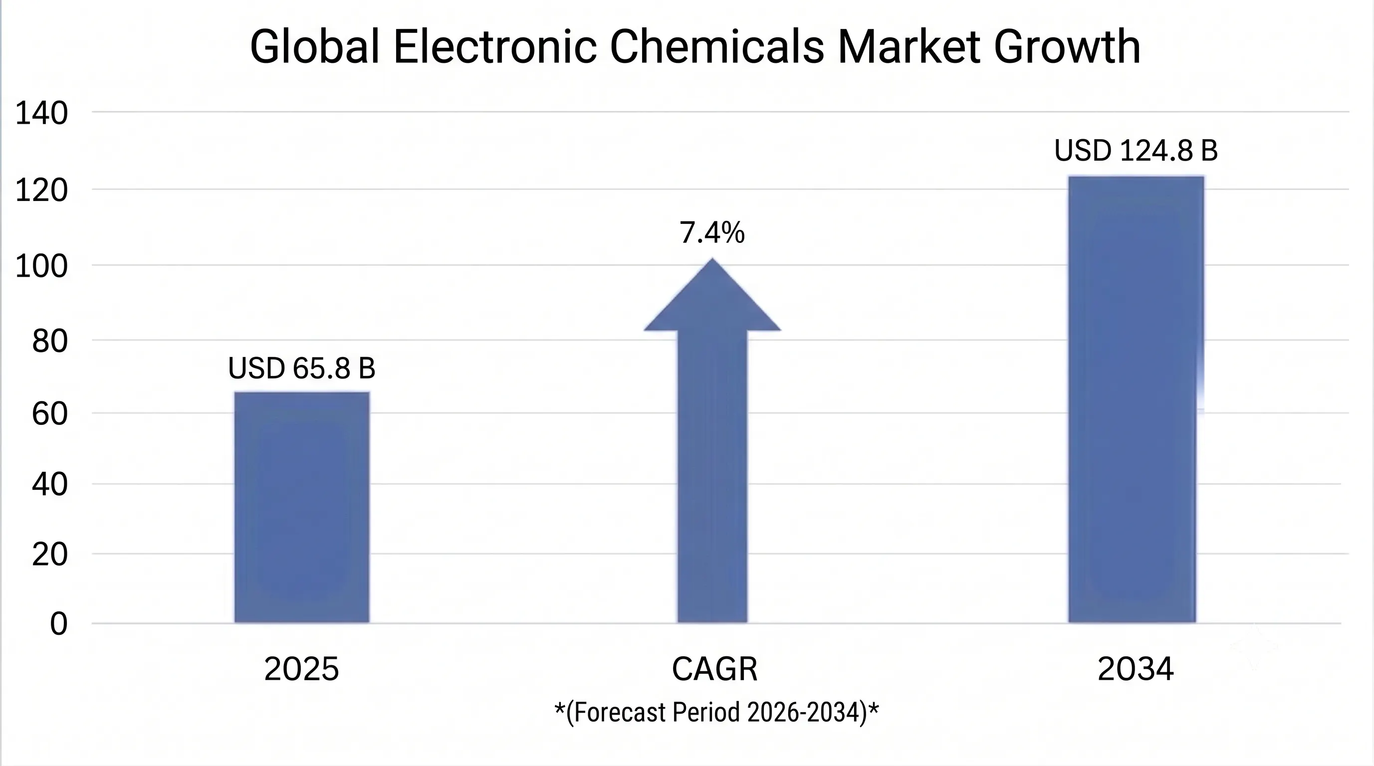
The global electronic chemicals market size was valued at USD 65.8 billion in 2025 and is projected to reach USD 70.2 billion in 2026, expanding to USD 124.8 billion by 2034, growing at a CAGR of 7.4% during the forecast period (2026-2034).
Electronic chemicals represent a highly specialized category of ultra-pure materials, gases, and advanced chemical formulations that serve as the fundamental building blocks for modern semiconductor manufacturing, electronics assembly, and advanced packaging processes. These materials operate under the most stringent purity requirements in the chemical industry, with contamination tolerances measured in parts per trillion for critical applications, as even microscopic impurities can cause catastrophic device failures in advanced semiconductor nodes below 3 nanometers. The market encompasses sophisticated chemical platforms including extreme ultraviolet photoresists enabling sub-7nm lithography, chemical mechanical planarization slurries achieving atomic-level surface planarity, specialty gases for precise doping and deposition processes, and ultra-pure wet chemicals for critical cleaning and etching applications.
The technological complexity of electronic chemicals has intensified dramatically as semiconductor manufacturing transitions from planar transistor architectures to three-dimensional structures including FinFET and Gate-All-Around designs, while simultaneously advancing to extreme ultraviolet lithography, multi-patterning techniques, and heterogeneous integration through advanced packaging. Each generational node transition requires entirely new chemical formulations optimized for smaller feature sizes, novel materials integration, and increasingly complex process flows that can involve over 1,000 individual processing steps per wafer. The market serves diverse applications beyond traditional semiconductors, including high-density printed circuit boards, flat panel displays utilizing OLED and microLED technologies, photovoltaic cells incorporating advanced heterojunction architectures, and emerging wide-bandgap power electronics based on silicon carbide and gallium nitride substrates.
The commercial ecosystem extends far beyond traditional chemical supply relationships to encompass comprehensive technical partnerships with semiconductor manufacturers, equipment vendors, and research institutions. Electronic chemical suppliers maintain dedicated on-site technical teams at major fabrication facilities, co-develop next-generation formulations aligned with customer technology roadmaps, and invest in specialized manufacturing infrastructure including ultra-clean production facilities, advanced analytical capabilities, and global distribution networks capable of maintaining chemical integrity throughout the supply chain. The market’s strategic importance has been amplified by geopolitical considerations, as governments worldwide recognize electronic chemicals as critical materials for semiconductor supply chain security, leading to substantial investments in domestic production capabilities and supply chain localization initiatives.
| Report Coverage | Details |
|---|---|
| Base Year | 2025 |
| Base Year Value | USD 65.8 Billion |
| Forecast Value | USD 124.8 Billion |
| CAGR | 7.4% |
| Forecast Period | 2025-2034 |
| Historical Data | 2022-2025 |
| Largest Market | Asia Pacific |
| Fastest Growing Market | North America |
| Segments Covered | By Product Type, Application, Process, End-User, Region |
| Region Covered | North America, Europe, Asia Pacific, Middle East & Africa, Latin America |
| Countries Covered | US, Canada, Mexico, Germany, UK, France, Italy, Netherlands, Japan, South Korea, Taiwan, China, Singapore, India, Israel, Brazil, UAE, Saudi Arabia |
| Key Market Playes | Merck KGaA, Shin-Etsu Chemical, JSR Corporation, Entegris Inc., BASF SE, Tokyo Ohka Kogyo, DuPont, Air Liquide, Linde plc, CMC Materials |
Get more details on this report - Request Free Sample
The primary structural driver propelling electronic chemicals market expansion is the unprecedented wave of semiconductor fabrication capacity investments worldwide, catalyzed by government initiatives including the USD 52.7 billion US CHIPS and Science Act, the EUR 43 billion European Chips Act, and similar programs across Asia-Pacific nations seeking to establish domestic semiconductor manufacturing capabilities. These initiatives have triggered over USD 300 billion in announced semiconductor facility investments between 2022 and 2026, with each leading-edge fabrication facility consuming USD 120-200 million in electronic chemicals annually at full production capacity. The transition to advanced semiconductor nodes below 5 nanometers has fundamentally altered chemical consumption patterns, with next-generation processes requiring 40-60% more chemical process steps per wafer compared to 28nm technologies due to increased complexity in lithography, etching, deposition, and planarization operations.
Advanced node manufacturing demands entirely new categories of electronic chemicals, including extreme ultraviolet photoresists formulated for 13.5nm wavelength radiation, metal-containing resists for enhanced sensitivity and resolution, atomic-layer etching precursors enabling precise material removal at the atomic scale, and specialized chemical mechanical planarization formulations capable of achieving sub-angstrom surface uniformity across 300mm wafers. The commercial impact extends beyond volume growth to encompass premium pricing for advanced formulations, with EUV photoresists commanding USD 8,000-15,000 per kilogram compared to USD 800-1,200 for conventional 193nm resists, reflecting the extraordinary technical complexity and stringent purity requirements of leading-edge applications.
The semiconductor industry’s evolution toward heterogeneous integration through advanced packaging architectures including 2.5D interposers, 3D IC stacking, and chiplet-based designs creates additional chemical consumption streams beyond traditional wafer fabrication. Advanced packaging processes require specialized materials for through-silicon via formation, redistribution layer patterning, hybrid bonding surface preparation, and encapsulation applications, with the advanced packaging chemicals market growing at 14.6% annually, significantly outpacing overall market growth rates.
The global automotive industry’s accelerating transition to battery electric vehicles and hybrid powertrains has created substantial incremental demand for power semiconductors, advanced driver assistance systems, and in-vehicle networking components, each manufactured using specialized electronic chemicals. Electric vehicle production reached 17.4 million units in 2025, representing 19.8% of total passenger vehicle production, with projections indicating 38-42 million units annually by 2030. Each electric vehicle incorporates 800-1,200 individual semiconductor devices compared to 400-600 in conventional vehicles, with autonomous driving-capable platforms containing over 3,000 chips, creating a compound demand multiplier for electronic chemicals serving automotive semiconductor manufacturing.
Power electronics based on wide-bandgap materials including silicon carbide and gallium nitride represent a particularly dynamic growth segment, with silicon carbide content per electric vehicle averaging USD 350-500 in 2025 compared to USD 50-80 in conventional internal combustion vehicles. The fabrication of wide-bandgap devices requires specialized chemical processes distinct from traditional silicon manufacturing, including tailored chemical mechanical planarization slurries optimized for the extreme hardness of silicon carbide substrates, selective etchants for gallium nitride epitaxial layers, and high-temperature-stable cleaning chemistries capable of maintaining performance at elevated processing temperatures required for wide-bandgap materials.
The automotive semiconductor supply chain imposes additional requirements for electronic chemicals including extended temperature cycling qualifications, enhanced reliability testing, and zero-defect quality standards that exceed those of consumer electronics applications. These requirements drive premium pricing for automotive-qualified chemical formulations and create barriers to entry that benefit established suppliers with comprehensive automotive qualification programs and manufacturing systems certified to automotive quality standards.
The rapid deployment of artificial intelligence applications, machine learning workloads, and high-performance computing infrastructure has created unprecedented demand for advanced logic processors, high-bandwidth memory devices, and specialized accelerators, each requiring sophisticated electronic chemicals for manufacturing. AI data centers and cloud computing facilities consume processors manufactured using the most advanced semiconductor nodes available, typically 3nm and below, which demand the highest-performance electronic chemicals including next-generation EUV photoresists, ultra-selective atomic-layer etching formulations, and advanced interconnect materials capable of supporting high-frequency signal transmission with minimal loss.
High-bandwidth memory production, essential for AI accelerators and graphics processors, requires specialized chemical processes for 3D NAND flash integration, through-silicon via formation, and multi-die stacking applications. The manufacturing complexity of high-bandwidth memory devices involves over 1,500 individual process steps per device, compared to 800-1,000 steps for conventional memory products, creating proportionally higher chemical consumption per unit of production capacity. The market benefits from premium pricing for AI-optimized semiconductor devices, which typically command 2-3 times higher average selling prices compared to conventional processors, enabling semiconductor manufacturers to justify premium costs for advanced electronic chemicals that enhance device performance and manufacturing yield.
The electronic chemicals industry exhibits significant geographic and supplier concentration that creates systemic vulnerabilities to geopolitical tensions, trade restrictions, and supply chain disruptions. Japan controls approximately 70-80% of global photoresist production capacity, with three companies - JSR Corporation, Tokyo Ohka Kogyo, and Shin-Etsu Chemical - collectively dominating advanced photoresist supply for leading-edge semiconductor applications. This concentration became acutely problematic during Japan’s 2019 export restrictions on fluorinated polyimides, photoresists, and hydrogen fluoride to South Korea, which disrupted Korean semiconductor manufacturers and demonstrated the fragility of concentrated specialty chemical supply chains.
The implementation of comprehensive export control regimes by the United States Bureau of Industry and Security since 2022 has created additional complexity for electronic chemical suppliers, restricting the supply of certain advanced formulations to Chinese semiconductor manufacturers while requiring extensive compliance programs and dual supply chain management. These restrictions have accelerated Chinese government investment in domestic electronic chemicals development, though Chinese suppliers remain significantly behind global technology leaders in advanced node chemical capabilities, particularly for EUV photoresists and atomic-layer processing materials.
The supply chain concentration extends beyond photoresists to encompass specialty gases, ultra-pure wet chemicals, and advanced packaging materials, where limited supplier bases create single-source dependencies for critical manufacturing inputs. Natural disasters, facility accidents, or geopolitical disruptions affecting key production sites can create industry-wide supply shortages with limited short-term alternatives, as demonstrated by various incidents including the 2011 tsunami impact on Japanese chemical facilities and COVID-19 disruptions to global logistics networks.
Per- and polyfluoroalkyl substances, commonly known as PFAS, have been extensively utilized in electronic chemical formulations including photoresists, cleaning agents, etchants, and surface treatment chemicals due to their exceptional chemical stability, surface energy properties, and process performance characteristics. Regulatory agencies across the United States, European Union, and multiple Asian jurisdictions are implementing comprehensive PFAS restrictions that require reformulation of numerous established electronic chemical products, creating significant technical and commercial challenges for suppliers and semiconductor manufacturing customers.
The European Union’s universal PFAS restriction proposal, under evaluation through the REACH regulation framework, could affect over 200 electronic chemical formulations currently used in semiconductor manufacturing and requiring substitute chemistries that must undergo extensive qualification testing at customer fabrication facilities before commercial adoption. Semiconductor facility qualification of new chemical formulations typically requires 12-24 months and USD 5-15 million in testing and validation costs per product, creating substantial switching costs and extended transition timelines that complicate regulatory compliance efforts.
The technical challenge of PFAS substitution extends beyond simple chemical replacement to encompass fundamental reformulation of products that have been optimized over decades for specific performance characteristics. Alternative chemistries may exhibit different process behaviors, require modified equipment settings, or deliver inferior performance compared to PFAS-containing formulations, potentially impacting manufacturing yields and device reliability. The industry faces the challenge of maintaining performance standards while meeting environmental regulations, often requiring substantial research and development investments with uncertain commercial outcomes.
Government-driven semiconductor supply chain localization initiatives worldwide have created compelling opportunities for electronic chemical manufacturers to establish regional production facilities near new semiconductor fabrication sites, capturing preferential supplier relationships, reduced logistics costs, and strategic partnerships with government-backed manufacturing programs. The US CHIPS and Science Act specifically identified electronic chemicals as critical supply chain vulnerabilities, with dedicated funding streams supporting domestic materials production capacity development. Major electronic chemical suppliers including Entegris, CMC Materials, Merck KGaA, and BASF have announced North American capacity expansions totaling over USD 3.2 billion between 2023 and 2027.
The opportunity extends beyond simple capacity replication to encompass development of regionally optimized supply chains with reduced lead times, enhanced technical support proximity, and greater supply security that commands premium pricing from semiconductor manufacturers prioritizing supply chain resilience over cost optimization. Electronic chemical suppliers establishing co-location or near-location manufacturing adjacent to major fabrication clusters in Arizona, Ohio, Texas, and Germany are positioned to capture long-term preferred supplier agreements with new facility operators seeking to minimize supply chain risk and ensure continuous material availability.
Regional manufacturing initiatives also enable closer collaboration between chemical suppliers and semiconductor manufacturers in developing next-generation formulations optimized for specific process requirements, equipment configurations, and product specifications. This collaborative approach accelerates innovation cycles, reduces qualification timelines, and creates competitive advantages for suppliers with strong local technical capabilities and manufacturing flexibility.
The semiconductor industry’s strategic shift toward advanced packaging architectures including chiplets, 2.5D and 3D integration, fan-out wafer-level packaging, and hybrid bonding has created substantial new demand for specialized electronic chemicals serving packaging processes that were previously considered less technically demanding than front-end wafer fabrication. Advanced packaging now accounts for approximately 30-35% of total semiconductor manufacturing value, with chemical consumption growing proportionally as packaging complexity increases through multi-die integration, through-silicon via interconnects, and micro-bump bonding processes requiring nanometer-scale precision.
Hybrid bonding technology, which enables direct copper-to-copper interconnects at pitches below 10 micrometers for stacked memory and logic integration, requires ultra-high-purity copper plating chemistries, surface activation treatments, and cleaning formulations with contamination specifications approaching those of leading-edge front-end processes. The development of hybrid bonding-compatible chemical platforms represents a significant commercial opportunity, with the technology enabling new product categories including high-bandwidth memory stacks, chiplet-based processors, and advanced sensor integration architectures.
The advanced packaging chemical market encompasses diverse application areas including redistribution layer patterning using specialized photoresists, underfill materials for thermal and mechanical protection, encapsulation compounds for environmental isolation, and temporary bonding adhesives for wafer-level processing. Each application area demands tailored chemical formulations optimized for specific thermal, mechanical, and electrical requirements, creating opportunities for suppliers with comprehensive materials science capabilities and advanced packaging expertise.
The electronic chemicals industry is experiencing a fundamental transformation toward sustainable chemistry principles, driven by environmental regulations, corporate sustainability commitments, and customer demands for reduced environmental impact throughout the semiconductor manufacturing lifecycle. Leading electronic chemical suppliers are investing substantially in developing environmentally benign alternatives to traditional formulations, including low global warming potential specialty gases, biodegradable cleaning chemistries, and recyclable packaging materials that maintain performance while reducing environmental footprint.
The development of circular economy approaches within electronic chemicals encompasses solvent recovery and recycling systems, chemical reclaim programs for high-value materials, and waste stream valorization technologies that convert manufacturing byproducts into useful chemical feedstocks. Advanced analytical capabilities enable real-time monitoring of chemical purity and composition throughout recycling processes, ensuring that reclaimed materials meet stringent semiconductor manufacturing specifications while reducing virgin material consumption and waste generation.
Sustainability initiatives extend to manufacturing process optimization through artificial intelligence and machine learning platforms that minimize chemical consumption, reduce energy requirements, and optimize yield rates across production operations. These technologies enable predictive maintenance of chemical delivery systems, real-time process optimization based on environmental conditions, and automated quality control systems that reduce material waste while maintaining product specifications.
Electronic chemical suppliers and semiconductor manufacturers are increasingly deploying artificial intelligence and machine learning platforms to optimize chemical formulation development, process control, and defect prediction, accelerating development cycles while improving process consistency and manufacturing yield. AI-driven formulation design platforms analyze vast experimental datasets to identify optimal chemical compositions, additive concentrations, and process parameters that would otherwise require years of empirical testing through conventional approaches, compressing development timelines from 3-5 years to 12-18 months for certain chemical product categories.
In-line process control applications utilize machine learning models trained on process sensor data, chemical concentration measurements, and wafer metrology results to predict and prevent process excursions before they generate defective products, reducing chemical waste and improving manufacturing efficiency. Leading semiconductor manufacturers including TSMC, Samsung, and Intel have reported 15-25% reductions in chemical process variability through AI-assisted process control implementations, translating directly into improved device yields and reduced chemical consumption per functional device.
Predictive analytics platforms enable anticipatory supply chain management through demand forecasting models that incorporate semiconductor industry cycles, technology roadmaps, and macroeconomic indicators to optimize inventory levels, production planning, and distribution logistics. These systems reduce supply chain disruptions, minimize inventory carrying costs, and improve customer service levels through proactive capacity allocation and strategic stock positioning.
Asia Pacific commands the largest market share of approximately 68%, valued at USD 44.8 billion in 2025, reflecting the region’s commanding position in global semiconductor manufacturing with Taiwan, South Korea, Japan, and China collectively accounting for over 75% of global semiconductor production value. Taiwan Semiconductor Manufacturing Company alone, operating the world’s most advanced logic foundry with leading-edge 3nm production, consumes electronic chemicals at a scale that positions Taiwan as the single largest national market for advanced photoresists, CMP slurries, and specialty gases. The company’s planned expansion to 2nm production and advanced packaging capabilities will drive incremental chemical demand exceeding USD 800 million annually by 2027.
South Korea’s Samsung Electronics and SK Hynix represent the dominant demand centers for memory-specific electronic chemicals, including tungsten CMP slurries for 3D NAND manufacturing and specialized etchants for DRAM capacitor formation. The transition to 200+ layer 3D NAND architectures and next-generation DRAM technologies including DDR5 and LPDDR5X creates substantial incremental chemical consumption through increased process complexity and higher material consumption per device.
Japan occupies a unique position as both a major electronic chemicals producer and consumer, hosting global headquarters of leading suppliers including Shin-Etsu Chemical, JSR Corporation, Tokyo Ohka Kogyo, and Fujifilm while maintaining significant domestic semiconductor manufacturing through companies including Sony Semiconductor Solutions and Renesas Electronics. The Japanese government’s strategic investment in attracting TSMC’s Kumamoto facility and supporting domestic semiconductor revival through the Rapidus initiative targeting 2nm production by 2027 creates incremental domestic chemical demand alongside Japan’s established supplier ecosystem.
North America represents the fastest-growing regional market, with a projected CAGR of 11.2% through 2034, reaching USD 18.6 billion from USD 7.8 billion in 2025., driven by unprecedented semiconductor manufacturing investment catalyzed by the CHIPS and Science Act and strategic supply chain reshoring initiatives. The construction of TSMC’s Arizona facilities, Intel’s Ohio and Arizona expansions, Samsung’s Texas fabrication facility, and Micron’s Idaho and New York investments represents the largest concentration of new semiconductor manufacturing capacity in North American history, creating proportional demand growth for all categories of electronic chemicals.
The regional market benefits from a developing ecosystem of electronic chemical suppliers establishing or expanding North American production to serve new fabrication customers, government incentives supporting domestic materials manufacturing, and strategic imperatives from semiconductor manufacturers to diversify supply chains away from Asia-concentrated sources. Major suppliers including Entegris, CMC Materials, BASF, and Merck KGaA have collectively announced over USD 2.8 billion in North American electronic chemical manufacturing investments between 2023 and 2026, with facilities strategically located near major semiconductor clusters to minimize logistics costs and supply chain risks.
The market transformation encompasses both volume growth and supply chain localization, with semiconductor manufacturers willing to pay premium pricing for domestically sourced electronic chemicals that provide supply security, reduced lead times, and enhanced technical support proximity. Government funding through the CHIPS Act specifically supports domestic electronic chemical supply chain development, with USD 2.8 billion allocated for materials and chemicals infrastructure development.
CMP Slurries & Pads represent the largest product segment at 28% market share valued at USD 18.4 billion in 2025, growing at 8.6% CAGR through 2034. Chemical mechanical planarization slurries are abrasive chemical formulations used to achieve atomic-level surface planarity between semiconductor processing steps, with formulations specifically tailored for different materials including copper interconnects, tungsten plugs, silicon dioxide dielectrics, silicon nitride barriers, and advanced low-k dielectric films. The segment benefits from increasing process step counts at advanced nodes, premium pricing for leading-edge formulations, and growing adoption in advanced packaging applications requiring precise surface preparation for hybrid bonding and through-silicon via formation.
Photoresists & Ancillaries account for 22% market share at USD 14.5 billion in 2025, encompassing deep ultraviolet, extreme ultraviolet, and electron beam resist formulations used in lithographic patterning processes. The segment commands the highest average selling prices in the electronic chemicals market, with EUV photoresists priced at USD 8,000-15,000 per kilogram compared to USD 800-1,200 per kilogram for conventional 193nm resists, reflecting the extreme technical complexity and purity requirements of EUV-compatible formulations designed for sub-7nm device manufacturing.
Specialty Gases represent 18% market share at USD 11.8 billion in 2025, including ultra-high-purity gases used for deposition, etching, doping, and cleaning applications throughout semiconductor manufacturing. The segment encompasses carrier gases, reactive gases, and precursor chemicals delivered in specialized packaging systems that maintain purity and prevent contamination during storage and delivery to process tools.
Semiconductor & IC Manufacturing dominates application segments at 72% market share valued at USD 47.4 billion in 2025, growing at 8.4% CAGR through 2034. This segment encompasses the complete range of electronic chemicals consumed in wafer fabrication, from front-end transistor formation through back-end interconnect formation and advanced packaging applications. The segment benefits from leading-edge node transitions increasing chemical complexity and consumption, global fabrication capacity expansion, and premium pricing for advanced node formulations that enable next-generation device performance.
Printed Circuit Boards account for 12% market share at USD 7.9 billion in 2025, consuming specialized chemicals for substrate preparation, copper plating, solder mask application, and surface finishing processes. The segment serves diverse end markets including consumer electronics, automotive systems, telecommunications infrastructure, and industrial equipment requiring high-density interconnect solutions.
Flat Panel Displays represent 8% market share at USD 5.3 billion in 2025, utilizing photoresists, etchants, and cleaning chemicals in the production of LCD, OLED, and emerging microLED panels for consumer electronics, automotive displays, and professional monitor applications.
Consumer Electronics represents the largest end-use segment at 38% market share, driven by smartphones, tablets, personal computers, and wearable devices incorporating advanced logic and memory semiconductors manufactured using leading-edge electronic chemicals. The segment benefits from continuous device performance improvements requiring advanced semiconductor nodes and sophisticated packaging technologies.
Automotive Electronics is the fastest-growing end-use segment at 14.8% CAGR through 2034, driven by electric vehicle adoption, autonomous driving system proliferation, and advanced driver assistance features increasing semiconductor content per vehicle. The segment demands automotive-qualified electronic chemicals meeting extended temperature cycling, enhanced reliability, and zero-defect quality standards.
Telecommunications accounts for 16% market share, serving 5G infrastructure deployment, data center expansion, and network equipment manufacturing requiring high-performance semiconductors and advanced packaging solutions.
The global electronic chemicals market exhibits moderate to high concentration in specialized product categories, with the top ten players controlling approximately 58-65% of total market value through comprehensive product portfolios, advanced manufacturing capabilities, and established customer relationships with leading semiconductor manufacturers. Competitive dynamics vary significantly across product segments, with photoresists and advanced CMP slurries demonstrating oligopolistic structures where three to four suppliers control the majority of leading-edge supply, while commodity wet chemicals and standard cleaning agents feature more fragmented competitive landscapes with regional producers competing primarily on cost and logistics efficiency.
Market leadership requires substantial investment in research and development, typically 8-12% of revenues, to maintain technology roadmaps aligned with semiconductor manufacturer process development schedules 3-5 years in advance. Leading suppliers differentiate through technical performance at advanced process nodes, demonstrated process integration expertise enabling co-development with customer engineers, manufacturing quality systems ensuring ultra-high purity and batch-to-batch consistency, and supply chain reliability including geographic diversification and strategic inventory programs.
The competitive landscape is being reshaped by geopolitical considerations and supply chain localization requirements, creating opportunities for regional suppliers and driving established global players to invest in distributed manufacturing capabilities. Government support for domestic electronic chemical production through programs like the CHIPS Act provides competitive advantages for suppliers willing to establish local manufacturing and technical support infrastructure.
March 2026: Entegris Inc. announced the commercial launch of its next-generation EUV photoresist underlayer materials platform, enabling improved pattern transfer fidelity for sub-2nm device manufacturing. The product received qualification approval from two leading Asian foundries and is projected to contribute USD 180 million in incremental annual revenue at full market adoption.
February 2026: Merck KGaA completed expansion of its Darmstadt electronic chemicals production facility, adding 35% capacity for semiconductor-grade specialty gases and precursor chemicals. The expansion specifically targets supply for European semiconductor facilities under the EU Chips Act investment program, with dedicated production lines for automotive-qualified formulations.
January 2026: CMC Materials received qualification approval for its silicon carbide CMP slurry platform from three major power semiconductor manufacturers, addressing the rapidly growing market for electric vehicle power electronics. The qualification covers 150mm and 200mm silicon carbide wafer processing with demonstrated 40% reduction in surface roughness compared to conventional slurries.
December 2025: BASF SE announced a USD 400 million investment in a new electronic chemicals production facility in Phoenix, Arizona, strategically located adjacent to TSMC’s Arizona fabrication complex. The facility will supply ultra-pure wet chemicals and specialized CMP formulations with projected operational startup in Q2 2028.
November 2025: Shin-Etsu Chemical announced commercial availability of its metal-oxide EUV photoresist platform based on tin-oxide chemistry, representing the first commercially qualified metal-containing EUV resist from a Japanese supplier. Initial customer qualifications are underway at leading-edge logic foundries with commercial production expected in Q3 2026.
You'll get the sample you asked for by email. Remember to check your spam folder as well. If you have any further questions or require additional assistance, feel free to let us know via-
+1 724 648 0810 +91 976 407 9503 sales@intellectualmarketinsights.com
15 Apr 2024
Intellectual Market Insights Research © 2026. All rights reserved.